Semiconductor Companies Will Get Pinched for Scarce Isotopes from These Suppliers
From the Tight Spreads substack.
In the context of next-generation semiconductor architecture, the integration of isotopically enriched materials marks a shift from structural scaling to material-level optimization. While natural materials are sufficient for traditional computing, the demands of AI and quantum processing require the elimination of “isotopic noise.”
Below you’ll find:
How this problem exists today.
Examples of which semiconductor companies will benefit from isotopes that are produced by Oklo and ASPI.
It’s important to note both ASPI and Oklo have publicly stated entering definitive contracts / partnerships with semiconductor companies today.
Refer to: Isotopes 101 for technical context and Oklo’s Atomic Alchemy for the cross-conclusion on an INTC partnership. An ASPI version is next.
In nature, even a 100% chemically pure silicon wafer is an “isotopic soup” of three different versions (Si-28, Si-29, Si-30). They behave the same chemically, but their different masses and magnetic properties create three specific “noise” problems for AI that can enhance the chip by using more precise isotopic versions:
Thermal Noise (The Speed Bump): AI chips generate massive heat. In natural silicon, different isotopes have different masses, which act like speed bumps for heat vibrations (phonons). By using a single isotope like Silicon-28 from ASPI, the material becomes a perfectly smooth “track,” conducting heat 150% more effectively and allowing chips to run faster without melting.
Magnetic Noise (The Signal Blur): Natural silicon contains Si-29, which has a “nuclear spin” that acts like a tiny, flickering magnet. This “hum” interferes with the qubits in quantum computers (decoherence), but in high-speed AI chips, it creates signal jitter, forcing the system to waste up to 30% of its power on error correction.
Kinetic Noise (The Timing Jitter): At ultra-high frequencies (like 6G), minuscule mass differences between isotopes cause electrons to move at slightly different speeds. This creates “lags” in data timing. Eliminating these variations ensures every atom reacts to electricity with the exact same momentum, maintaining perfect data synchronization.
This is why companies like ASPI and Oklo’s Atomic Alchemy are vital. Traditional chemistry can’t fix this problem because you can’t “chemically” separate silicon from silicon. You need atomic separation (centrifuges, lasers, or reactors) to filter out the “heavy” atoms and leave behind a perfectly quiet, perfectly smooth material.
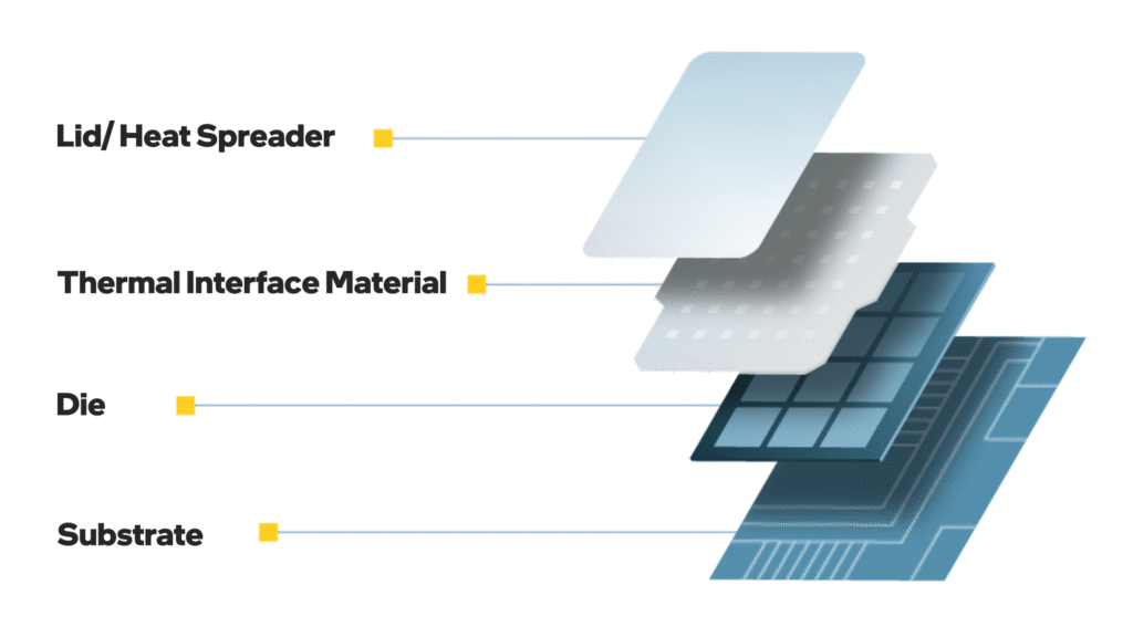
The Isotopically Engineered Chip Stack
1. Architecture & Design (The Blueprint)
This initial stage involves creating the logical and physical layout of the chip, defining how billions of transistors will interact, manage data flow, and dissipate heat to achieve target performance without physical failure.
The Body (Substrate): As the foundational floor, the substrate provides structural integrity and thermal grounding. NVIDIA architects can increase transistor density by planning for Silicon-28 substrates, which provide 1.5x better thermal conductivity than natural silicon to prevent AI chip meltdown.
Signal & Quantum Integrity: Qualcomm designers utilize Depleted Germanium-73 to remove “nuclear spin” noise for cleaner 6G signals. And for quantum computer bulls, IonQ and Quantinuum rely on Barium-137 and Ytterbium-171 as “cornerstone materials” to provide the long coherence times necessary for fault-tolerant quantum computing.
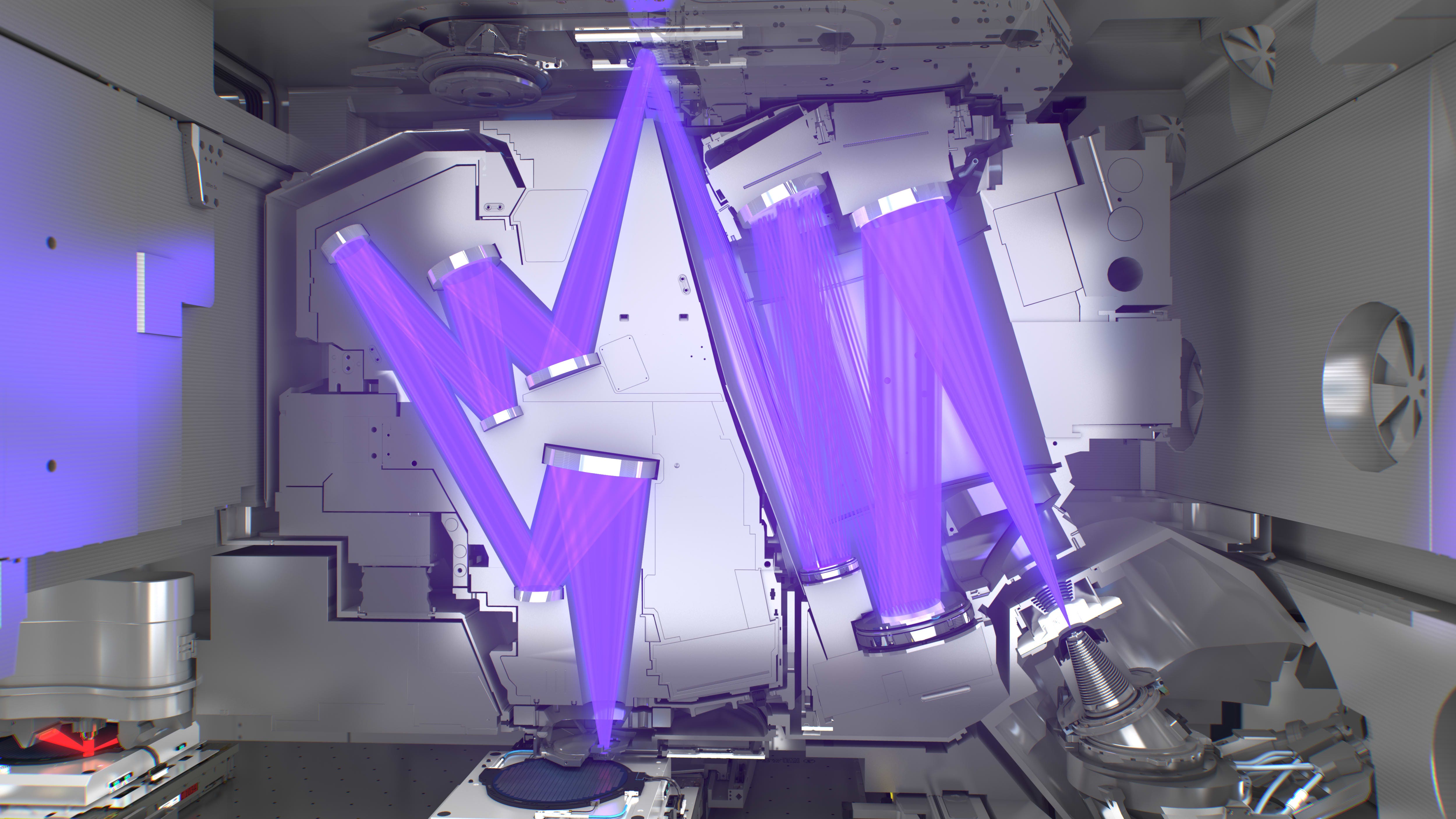
2. Equipment & Lithography (The Machinery)
This manufacturing stage focuses on providing the highly precise, specialized machines and ultra-pure materials required to physically “print” the intricate designs onto silicon wafers with atomic-level accuracy.
Enriched Silane: Unlike competitors who use complex chemical conversions, ASPI enriches Natural Silane Gas directly. This high-purity gas allows ASML and Applied Materials machines to deposit thin films with zero isotopic defects, maintaining the atomic integrity of sub-2nm nodes.
Vacuum Integrity: Enriched Krypton and Xenon isotopes are used as specialized buffer gases and leak detectors to maintain the ultra-vacuum environments essential for EUV (Extreme Ultraviolet) lithography systems.
ASML EUV lithography system:
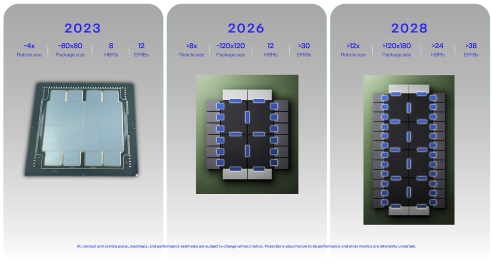
3. Fabrication (The Foundry)
The foundry is the “Engine Room” (Logic Layer) where the physical and nuclear properties of the chip are precisely set, transforming raw wafers into functional chips with billions of transistors.
Atomic Uniformity to Mitigate Error: Through Atomic Alchemy, Oklo irradiates silicon ingots with neutrons to create Phosphorus-31. This Neutron Transmutation Doping (NTD) achieves ultra-uniform electrical properties, preventing the hotspots and signal failures common in traditional doping for TSMC or Samsung high-power EV and industrial chips.
The 1nm Wall: As foundries move to Gate-All-Around architectures, they utilize ASPI’s Silicon-28 and Germanium-74 within the wafer itself. These isotopes serve as a “thermal highway” for tiny nanowires, significantly improving electron mobility and enabling the mass production of 1nm-class transistors.
Intel Foundry Design Roadmap:
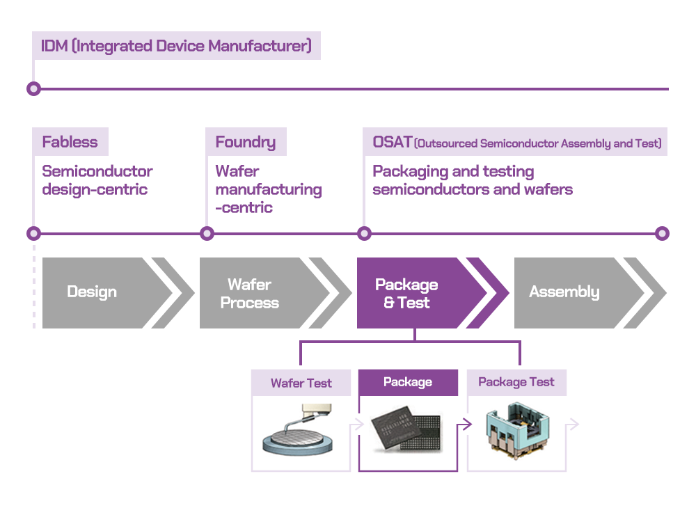
4. Outsourced Semiconductor Assembly and Test & Advanced Packaging
This final stage of production is responsible for the physical integration of multiple dies into a single package. It focuses on 3D stacking, creating high-speed electrical connections between layers, and managing the resulting “heat sandwich” to ensure long-term reliability.
Interconnect Signaling: Known as Through-Silicon Vias (TSVs), this section transports data between the logic core and the external world. By utilizing isotopically pure Silver-107 or 109 from ASPI, manufacturers like SK Hynix or Micron can eliminate “kinetic jitter,” ensuring the perfect signal timing required for HBM3 memory and 6G satellite arrays.
Mitigating heat sandwiches: In 3D-stacked AI chips, heat often gets trapped in the center of the stack. By integrating Silicon-28 into the packaging interposers, manufacturers create a thermal highway that pulls heat out of the stack (again, 1.5x faster than natural silicon) allowing for denser, more powerful configurations without thermal throttling.
The Sensing Layer: At the very top of the stack, the sensing layer acts as the chip’s interface with its environment. Using NMR-active isotopes like Thallium-204 and Phosphorus-31 (produced by Atomic Alchemy) along with Silver-107, engineers can “listen” to the chip’s internal health in real-time. These isotopes function as embedded diagnostic probes, detecting microscopic stress or electrical degradation before it leads to system failure.
Point in Process: